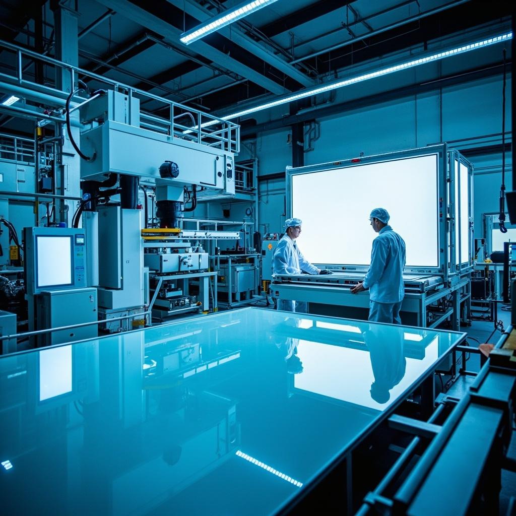
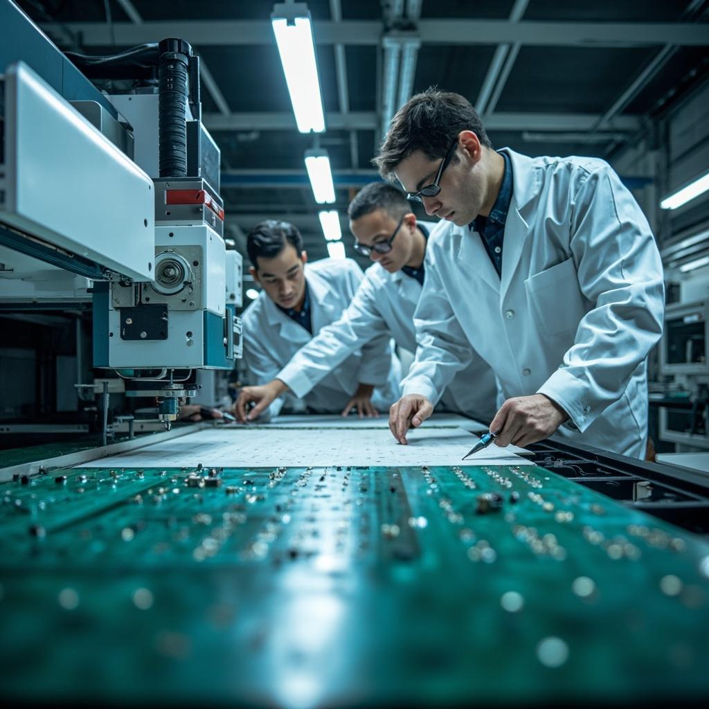
PCB fabrication equipment is a capital-intensive, technology-layered business where leadership is defined by process coverage rather than any single machine. A top-tier company must simultaneously master laser direct imaging (LDI) for fine-line patterning, mechanical and laser drilling for microvias, wet-process plating for hole metallization, and automated inspection for yield control. KLA, through its Orbotech brand, dominates the inspection and direct-imaging segment with roughly 10-micron defect capture and Triple Vision technology; MKS Instruments combines ESI laser drilling with Atotech plating chemistry to offer an integrated dry-plus-wet solution no rival fully replicates; and Han's CNC holds the world's largest mechanical drilling shipment share while pushing into CO2 and UV laser drilling.
Beyond technology, leadership requires global service density. PCB fabricators in China, Taiwan, Japan, Korea, and increasingly Thailand and Vietnam run equipment around the clock, so vendors must deploy application engineers and spare-parts logistics close to customers. Companies that merely sell machines without chemistry, software, or service ecosystems — a category this ranking excludes from the top tier — find their equipment commoditized as fabricators demand turnkey process solutions that guarantee yield, not just throughput.
Scale matters too. The firms ranked here generate from roughly $150 million to over $12 billion in annual revenue, and that capital base funds the R&D needed to keep pace with shrinking line widths and rising layer counts. A leading PCB equipment company in 2025-2026 combines process breadth, global service, and sustained R&D investment — the three pillars this ranking weighs most heavily.
As PCB line widths race toward 10 microns and layer counts climb past 30 for AI server boards, traditional contact lithography and mechanical-only drilling can no longer maintain yield. Direct imaging systems replace film-based exposure with laser scanning, cutting defects and supporting finer lines, while laser drilling — CO2 for blind vias and UV/picosecond lasers for microvias — replaces purely mechanical stacks in high-density interconnect (HDI) and IC substrate production.
The market data shows the shift clearly: global PCB laser drilling equipment reached approximately $1.8 billion in 2025 and is projected to double to about $3.6 billion by 2034, a compound annual growth rate near 8.1%. Direct imaging (LDI) is an even larger category, estimated at $2.44 billion in 2025 and headed toward $5.7 billion by 2035. Mitsubishi Electric leads CO2-laser drilling with machines capable of burning sub-50-micron blind vias at thousands of holes per second, while Han's CNC and its Shenzhen peers captured roughly 19% of newly added global laser drilling capacity in 2025.
For fabricators, the economic logic is compelling: laser and imaging upgrades lift yield, shorten cycle times, and enable higher-value products such as SLP and IC substrates. That is why capital expenditure in these two process steps absorbs the largest share of new equipment budgets and why the top-ranked companies in this list are precisely those with the strongest laser and imaging portfolios.
Artificial intelligence infrastructure is rewriting the specification sheet for PCB manufacturing equipment. AI server motherboards and switch backplanes demand 18 to 30+ layers, higher aspect-ratio microvias, and tighter impedance control — requirements that favor advanced laser drilling, vertical continuous plating (VCP), and high-end flying-probe testing. The result is an order boom for equipment vendors: Han's CNC revenue surged 72.7% in 2025, Dongwei Technology's PCB plating orders roughly doubled, and Mycronic set record order intake in Q2 2026 on the back of photonics and advanced substrate demand.
AI is also changing the buying criteria themselves. Fabricators now purchase whole process solutions rather than individual tools, seeking vendors who guarantee the interaction between laser drilling and subsequent copper plating chemistry. This favors vertically integrated players such as MKS Instruments, whose ESI lasers and Atotech chemistry share one process recipe; and it rewards vendors who embed AI into their own equipment, such as KLA's machine-learning-based defect classification and Nidec Advance Technology's AI-assisted optical inspection.
Capacity migration adds a second engine. As leading PCB makers relocate plants to Thailand, Vietnam, and Malaysia under China-Plus-One strategies, greenfield facilities order entire lines at once — a dynamic from which Chinese vendors like Han's CNC and Dongwei are capturing outsized share through aggressive pricing and rapid on-site service, while Japanese and European leaders defend the high-end substrate segment.
Inspection and electrical testing are the final gatekeepers of PCB quality, and this segment is dominated by a small group of specialists. KLA's Orbotech Ultra Dimension AOI systems set the reference for automated optical inspection, combining Triple Vision multi-image capture with 2D metrology to detect micro-scale defects on IC substrates and mSAP lines; the company's PCB and component inspection division generated roughly $622 million in revenue in fiscal 2025. In bare-board electrical testing, Sweden's Mycronic is the undisputed leader through its atg brand — its flying-probe and universal grid testers are the industry standard for high-reliability aerospace, medical, and server boards, with the new A9XL platform extending reach to oversized backplanes.
Japan's Nidec Advance Technology offers an alternative high-performance line: its GATS and SREC series testers handle advanced packaging substrates and large HDI boards, while the AURCA AI-based optical inspection series pushes automated defect classification. KLA, Mycronic, and Nidec collectively demonstrate that testing equipment is a high-margin specialty where process-knowledge depth — not scale alone — determines leadership.
For buyers, the practical takeaway is that inspection choices lock in yield outcomes. Because a single undetected micro short or open via can scrap an entire high-value substrate panel, leading fabricators standardize on two or three validated test platforms, creating durable vendor moats that this ranking recognizes in its testing-capability weighting.
Selecting PCB fabrication equipment is a multi-year capital decision, and the winning approach balances five factors. First, process coverage: prefer vendors whose portfolio spans imaging, drilling, plating, and testing so process interactions are managed by one accountable supplier — the model MKS Instruments built by unifying ESI lasers with Atotech chemistry. Second, total cost of ownership: compare not only machine price but chemistry consumption, maintenance intervals, and yield contribution; a $25 million MKS expansion in Guangzhou or a $25 million-plus gain in throughput from Han's CNC's laser drills can outweigh headline hardware costs.
Third, service proximity: with fabrication moving to Southeast Asia, vendors with local engineering staff and rapid spare-parts response — increasingly Han's CNC and Dongwei — reduce downtime risk versus suppliers requiring weeks-long international service visits. Fourth, technology roadmap: verify the vendor's investment in laser, AI inspection, and advanced-substrate capabilities, as these determine whether today's purchase remains competitive as line widths narrow. Finally, reference validation: audit installed-base performance at peer fabricators, since PCB equipment reputation is built on real factory yield data, not marketing claims.
This ranking treats these criteria as the practical filter separating the ten companies listed above from the dozens of regional machinery builders whose equipment, while capable, lacks the ecosystem depth, global service footprint, or R&D pipeline to guarantee long-term competitiveness in the AI era.