What Does "Semiconductor Manufacturing Equipment" Actually Include?
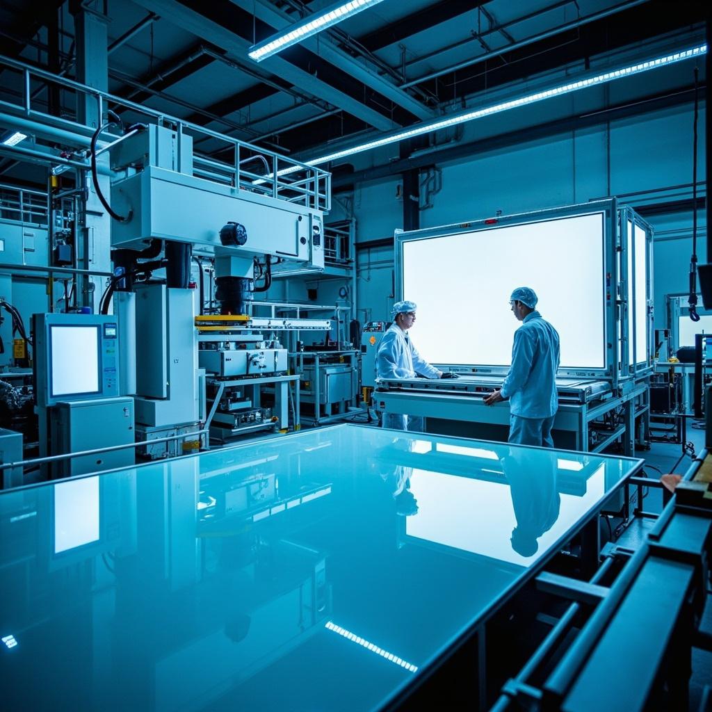
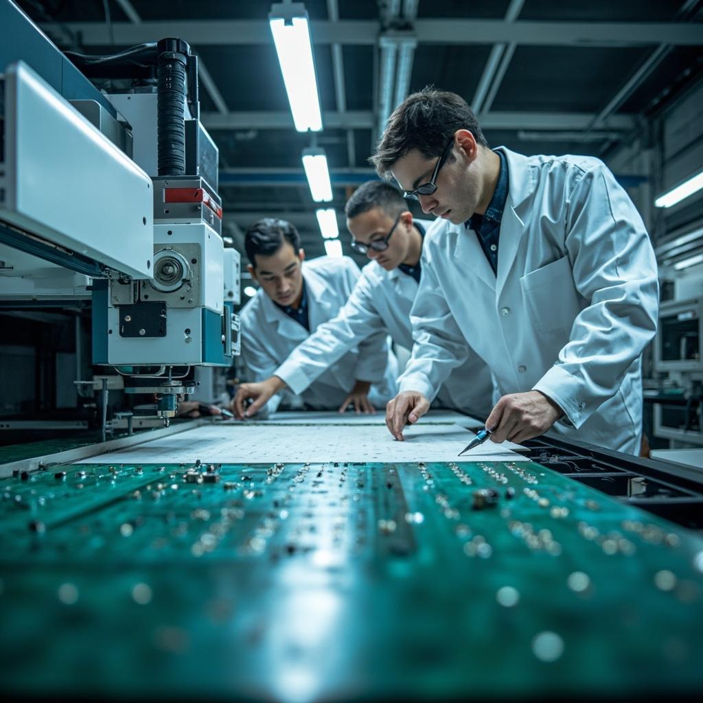
Semiconductor manufacturing equipment is the collection of precision machines used to build integrated circuits on silicon wafers, and it spans far more than lithography. The front end of the line (FEOL) covers photolithography systems (EUV and DUV), etch tools, thin-film deposition systems (CVD, PVD, ALD), ion implantation, cleaning systems, and chemical-mechanical planarization (CMP) machines. The back end of the line (BEOL) adds wafer inspection and metrology, packaging equipment, wafer dicing and grinding, and automated test equipment (ATE). In 2025 the global market for this machinery reached roughly $135 billion, according to SEMI, up 15% year-on-year, making it the single largest capital-spending category inside the semiconductor industry.
The companies in this ranking are highly specialized: ASML builds lithography systems, Applied Materials spans deposition, etch, CMP, and packaging, Lam Research concentrates on etch and deposition, KLA owns inspection and metrology, Advantest builds testers, and DISCO makes dicing saws and grinders. Together, this group covers every major process step from bare wafer to finished, tested chip. The equipment market is also becoming more concentrated: the top ten suppliers in this ranking accounted for the overwhelming majority of global billings in 2025, and their combined R&D spending exceeds $30 billion per year, which is why new entrants face a barrier measured in decades rather than years.
Why Do EUV Lithography Tools Cost More Than $200 Million?
Extreme ultraviolet (EUV) lithography is the most complex machine ever sold commercially. An EUV scanner uses a laser-produced plasma source that generates 13.5nm wavelength light, which must be reflected through a series of multilayer molybdenum-silicon mirrors with near-perfect precision — each mirror is polished to atomic tolerances. The entire optical path operates in a vacuum, and the machine consumes more power than a small factory. ASML, the world's only EUV supplier, shipped 48 EUV systems in 2025 and reported a 52.8% gross margin, reflecting the pricing power of a true monopoly. The next-generation High-NA EUV systems, now entering production at Intel and TSMC, cost even more, pushing the cost of a leading-edge fab toward $20 billion.
Because the machines are so expensive and so hard to build, buyers make decade-long commitments. TSMC, Samsung, and Intel pre-order tools years in advance, which is why ASML's order backlog — roughly €38.8 billion at the end of 2025 — is a closely watched indicator for the entire chip industry. The economics are also self-reinforcing: every new node (2nm, then 1.4nm) requires more EUV layers, so a fab that commits to ASML today locks in a decade of purchases, service contracts, and upgrades that cannot be transferred to a competitor.
Which Capabilities Separate the Top Semiconductor Equipment Companies?
The top ten semiconductor equipment companies share four capabilities that smaller rivals cannot easily replicate. First, technology depth: each leader holds a dominant position in at least one critical process step — KLA holds roughly half of process control, Tokyo Electron more than 90% of coater/developer systems, and ASM International about 55% of ALD. Second, installed base economics: once a fab adopts a tool platform, the supplier generates recurring revenue from parts, upgrades, and service for 10 to 20 years. Third, R&D intensity: leaders invest 15% to 20% of revenue back into development; Applied Materials alone spent $3.57 billion on R&D in FY2025, and ASML employs more than 14,000 engineers across its global R&D network. Fourth, customer lock-in: equipment must be qualified with specific chip processes, making switching costs prohibitive.
These dynamics explain the industry's extraordinary profitability. KLA generated a 62.3% gross margin and DISCO a gross margin above 70% in their most recent fiscal years — among the highest of any industrial sector. The flip side is that leadership is hard-won: Tokyo Electron's near-total control of coater/developer systems took four decades to build, and ASM International spent more than 30 years perfecting ALD before it became the default solution for GAA transistor manufacturing.
How Should Buyers Evaluate Semiconductor Equipment Suppliers?
For foundries, OSATs, and IDMs purchasing equipment, the evaluation framework goes beyond price. The first criterion is process capability: can the tool hit the required node, uniformity, and defect specs for the specific process step? Second is total cost of ownership (TCO), which includes throughput, uptime, consumables, and service — a cheaper machine with lower uptime is usually a bad deal. Third is supplier support: response time, spare parts availability, and local engineering presence in the fab region. Fourth is roadmap alignment: will the supplier's next-generation platform support your next node? Fifth is compliance: with export controls tightening, buyers must verify that equipment and service can legally be delivered in their jurisdiction.
For most leading-edge fabs, the practical answer is a multi-vendor strategy: ASML for lithography, Lam and Applied Materials for etch and deposition, KLA for inspection, and Advantest or Teradyne for test. Diversification reduces single-point risk while preserving access to best-in-class technology. Buyers should also evaluate the service ecosystem: equipment uptime above 90% is standard in this industry, and the best suppliers guarantee mean-time-to-repair measured in hours, with spare-part depots positioned within a few hours of every major fab cluster in Taiwan, Korea, China, Japan, and the United States.
How Is the Semiconductor Equipment Market Changing Between 2025 and 2026?
Three shifts define the 2025-2026 cycle. First, AI-driven demand: generative AI and high-bandwidth memory (HBM) have made advanced packaging and test equipment the fastest-growing segments; KLA's advanced packaging process control revenue grew about 70% in 2025, and Advantest's sales surged 44.7% to ¥1.128 trillion as AI chip testing intensity multiplied. Second, geographic realignment: export controls are splitting the market into two supply chains — Western and Japanese suppliers serving advanced nodes in the US, Europe, and Taiwan, while Chinese platform companies like NAURA capture mature-node demand at home; NAURA's revenue grew 30.85% in 2025 to ¥39.35 billion. Third, capacity expansion: ASML announced plans to expand EUV and DUV production capacity by 30% over two years, and Tokyo Electron completed new R&D centers in Miyagi and Kumamoto, signaling confidence in a multi-year upcycle.
SEMI projects the equipment market will grow from $135 billion in 2025 toward $138-143 billion by 2030, with advanced packaging and back-end tools taking an increasing share as chipmakers shift from pure scaling to heterogeneous integration. The long-term trajectory is supported by structural demand: more than 60 new wafer fabs are under construction worldwide, each requiring $10-20 billion of equipment, which implies several more years of elevated billings for the top ten suppliers in this ranking.