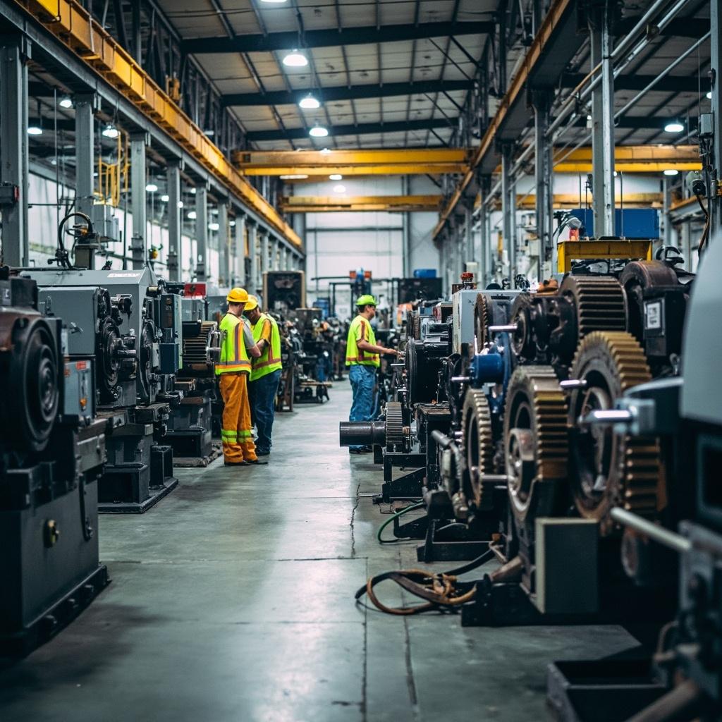
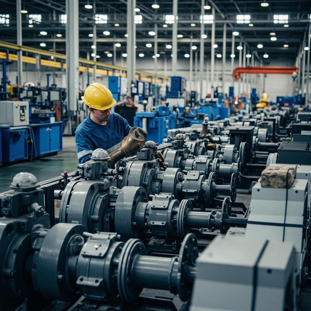
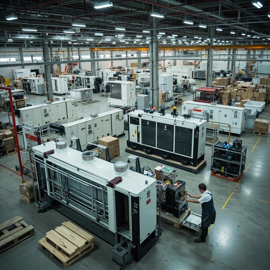
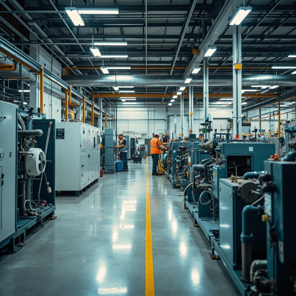
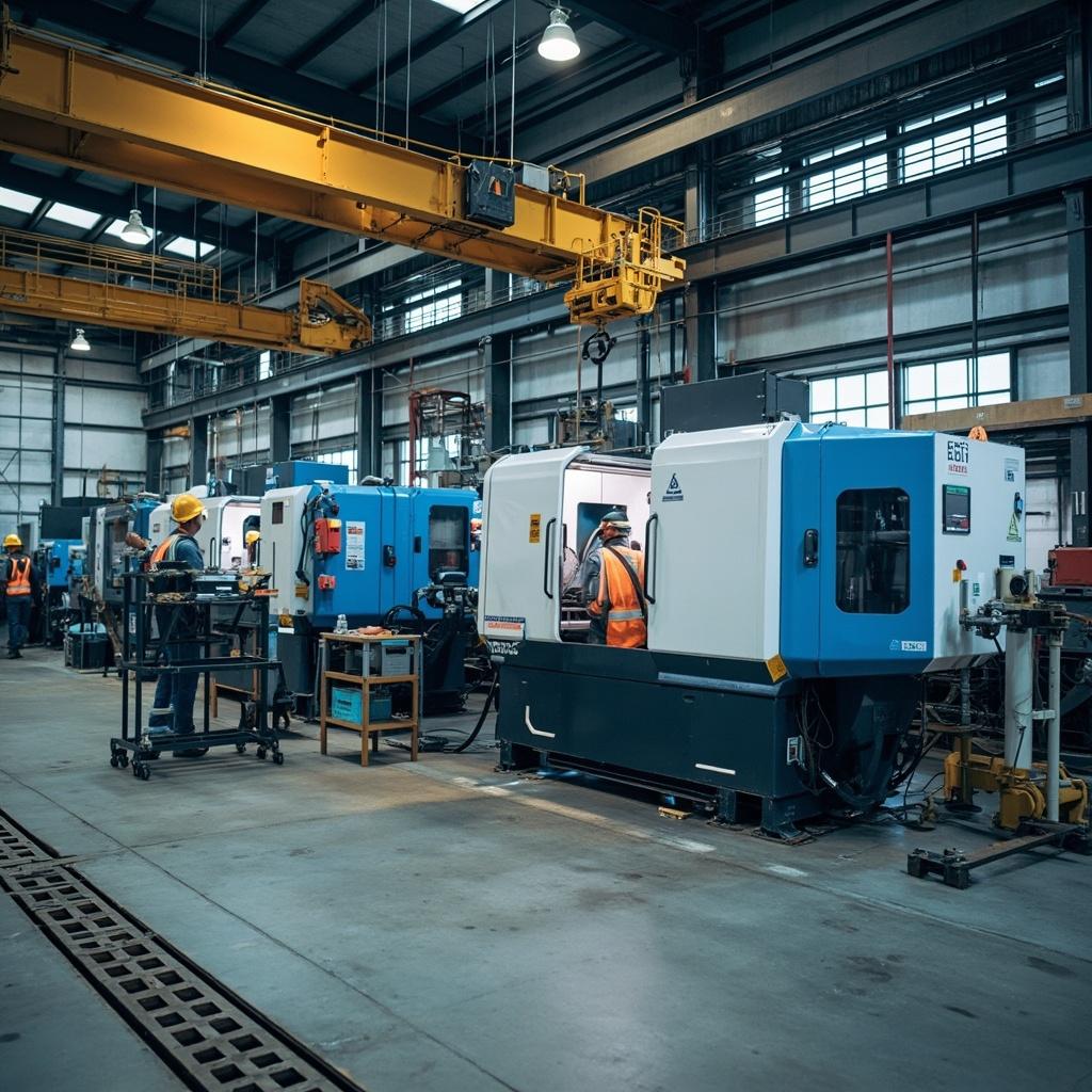
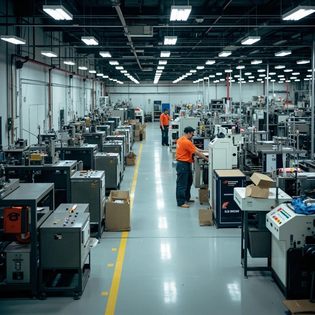
VerityRank scores semiconductor equipment manufacturers on physical manufacturing substance — the ability to build precision machines at scale — not brand marketing. The framework uses three weighted dimensions. Self-Manufacturing Depth & Production Scale carries 45%, the highest weight of any category we evaluate: we measure factory footprint, cleanroom capacity, annual tool output, and the degree of in-house production of critical components. ASML's Veldhoven campus — one of Europe's largest cleanroom facilities — and DISCO's Hiroshima and Nagano plants exemplify the scale required. Tokyo Electron's 30 Japan-based R&D and manufacturing sites, and SCREEN's Hikone cluster in Shiga Prefecture, demonstrate the deep domestic manufacturing networks that define the industry's leaders.
Category Production Share accounts for 35%: we evaluate each company's share of its specific equipment category — ASML's 100% of EUV, Tokyo Electron's 80%+ of coater/developers, KLA's 50%+ of process control, ASMI's 55%+ of ALD, SCREEN's 35%+ of cleaning, DISCO's 70%+ of dicing.
Brand Influence & Global Sales completes the framework at 20%: total revenue, profitability, customer adoption at TSMC, Samsung, and Intel, and global operational footprint. Companies that only brand-and-assemble, without proprietary manufacturing, are excluded entirely. Scores are normalized to a 0-100 scale using FY2025-FY2026 financial disclosures and factory-level public data.
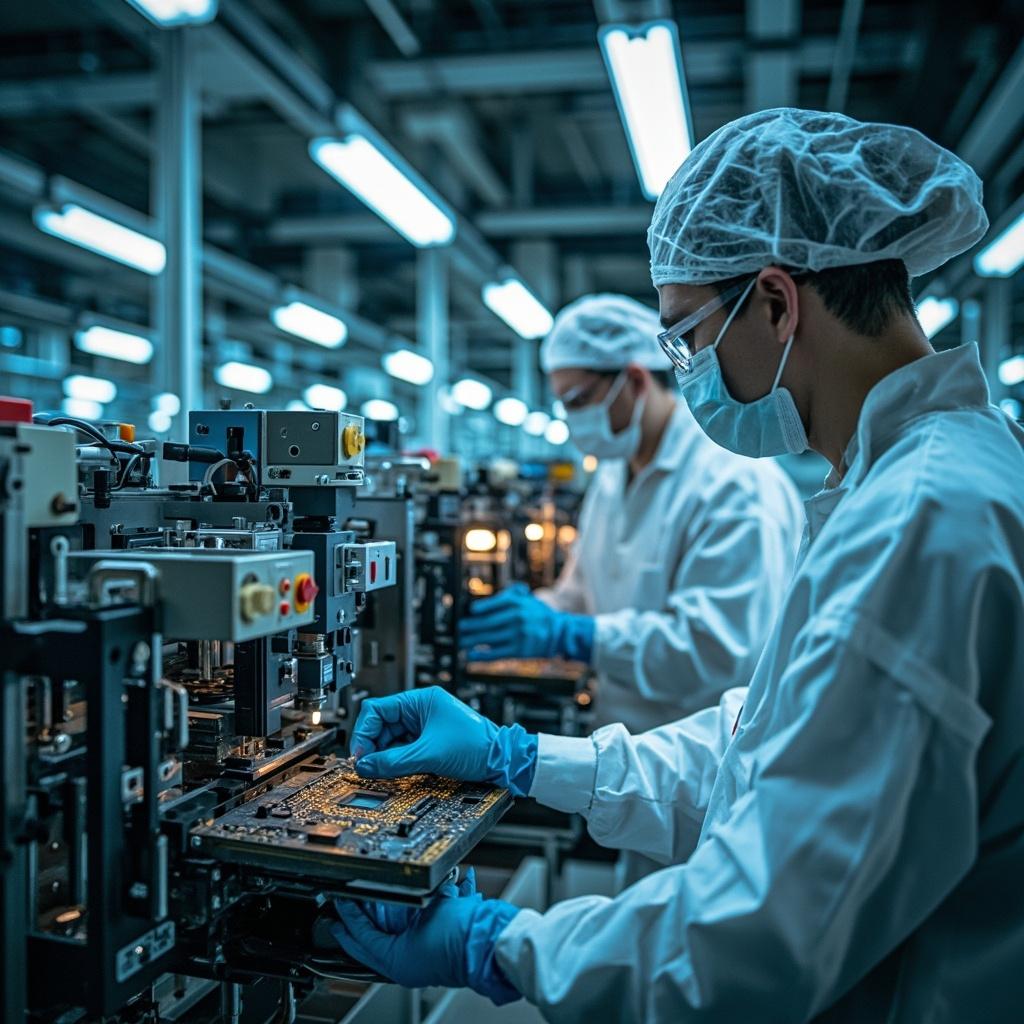
Five manufacturing capabilities separate genuine semiconductor equipment makers from assemblers — and the world's top ten all possess them at extraordinary depth. First, cleanroom assembly at scale: EUV systems, etch tools, and metrology platforms require class 10-100 cleanrooms where a single particle can destroy weeks of assembly. ASML's Veldhoven campus and Applied Materials' Austin and Santa Clara facilities operate some of the industry's largest cleanroom complexes. Second, precision component fabrication: superconducting magnets, optical columns, vacuum chambers, and high-speed displacement stages must be manufactured to nanometer tolerances — Tokyo Electron and SCREEN produce critical fluid-control and precision-motion components in-house in Japan.
Third, vertical integration of critical subsystems: the strongest manufacturers control their own RF power systems, gas delivery, optics, and process-control software — NAURA has deliberately cultivated a Chinese domestic supply chain of vacuum pumps, RF supplies, and precision chambers. Fourth,
global multi-site production: Lam Research operates plants in Fremont and Tualatin plus a mega-factory in Batu Kawan, Malaysia; ASMI concentrates high-volume manufacturing in Singapore and Dongtan, Korea. Fifth, process qualification infrastructure: every tool must be qualified at customer sites with months of process validation — this installed-base qualification, more than any patent, is what locks customers to a vendor for decades.
Semiconductor equipment is the most profitable manufacturing industry on earth because its customers cannot switch vendors without risking catastrophic yield loss. Gross margins tell the story: KLA and ASML sustain 52-62% gross margins, and DISCO exceeds 70% — levels normally associated with software, not hardware. The mechanism is the industry's astronomical switching costs. A modern fab line integrates tens of thousands of precision components and millions of lines of yield-control algorithms into a single interdependent system. When TSMC or Samsung installs a Tokyo Electron coater or a KLA inspection tool, the entire fab's process parameters are tuned around that equipment. Replacing a single tool means months of requalification and yield losses of tens of percentage points — unacceptable when a leading-edge wafer is worth thousands of dollars.
This creates monopoly-like pricing power in every category where one or two players dominate: ASML's 100% share of EUV, KLA's 50%+ of process control, DISCO's 70%+ of dicing, ASMI's 55%+ of ALD.
The equipment-plus-consumables model amplifies the moat: DISCO's cutting blades and grinding wheels, and SCREEN's cleaning chemicals, generate recurring high-margin revenue long after the initial tool sale. As chip architectures grow more complex — HBM, GAA, 3D NAND — the number of process steps and the inspection content per wafer grow faster than wafer production itself, continuously expanding the revenue pool available to these dominant manufacturers.
Geopolitics has become the single most powerful force reshaping semiconductor equipment manufacturing — redrawing supply chains, redirecting capital, and creating a new Chinese challenger. US export controls on advanced lithography, etch, and inspection tools to China have fundamentally altered revenue geography. ASML's China revenue is projected to shrink to about 20% of total in 2026, down from roughly 40% of bookings in 2024; Applied Materials' China share declined to 30%; and Tokyo Electron, KLA, and Lam Research all report tightening China access. In response, Western and Japanese manufacturers are building redundant, regionally distributed capacity — Tokyo Electron acquired an 87-acre Austin, Texas campus for $87 million, SCREEN opened a US R&D center in New York, and ASMI expanded manufacturing in Korea and Arizona.
The second-order effect is the rise of NAURA, China's platform champion: 2025 revenue of ¥39.35 billion, up 30.85%, with single-year recruitment of 4,747 new employees pushing headcount toward 15,000. NAURA is building a parallel domestic supply chain — vacuum pumps, RF power supplies, precision chambers — that no longer depends on Western components. Meanwhile, the AI boom is redirecting capital toward the US (CHIPS Act fab buildouts in Arizona, Texas, Ohio) and Europe, creating new manufacturing demand that partially offsets lost China business. The result is a
two-track industry: Western and Japanese leaders serving leading-edge fabs, and Chinese vendors consolidating domestic share while advancing toward international competitiveness.
AI is transforming semiconductor equipment demand from a cyclical business into a structural growth industry — with three distinct manufacturing consequences. First, leading-edge capacity expansion: AI accelerators and HBM memory are driving the largest fab buildout in history. Taiwan's equipment spending surged 90% in 2025, global billings hit $135 billion, and ASML's Q4 2025 orders reached a record €13.2 billion — €7.4 billion of EUV — as TSMC, Samsung, and Intel expand capacity for AI chips. Second, test content explosion: AI SoCs require far longer test times, and HBM stacks need extensive qualification. Advantest's FY2026 revenue jumped 45% to ¥1,129 billion with a 33.3% net margin — the highest in its history — as GPU and NPU test demand exceeded capacity. The company targets annual production of 5,000 advanced test systems.
Third, advanced packaging's manufacturing revolution: 2.5D/3D integration (HBM, chiplets) multiplies process steps — thin wafers, precise dicing, fine polishing, hybrid bonding. Applied Materials launched its
Kinex hybrid bonding system; KLA's advanced packaging yield-control revenue is doubling toward $1 billion; and DISCO's FY2026 sales hit a record ¥436.9 billion (+11.1%) as AI packaging demand drives ultra-thin die production. The AI era has converted the industry's manufacturing leaders — those with the deepest cleanroom capacity, most advanced process qualification, and strongest category monopolies — into structural beneficiaries of the largest technology investment cycle in history.